
How FPGAs use LUTs to replace Logic Gates
All about Look-Up Tables

In many undergraduate digital design courses, we are taught to think of logic gates as fixed circuits - hardwired, unchangeable, and fixed with a certain number of transistors. But inside an FPGA, the logic is far more flexible. Unlike ASICs, which are built off these gates, FPGAs' core building block is memory: the Look-Up Table or LUT. This small block of memory resides inside a Configurable Logic Block(CLB) and is in charge of implementing a combinational logic function. In this article, we will explore how LUTs work, how they are internally built, and the process of how the LUT runs, starting from your own Verilog code to the execution in hardware.
How the LUT runs
LUTs store precomputed outputs for all possible inputs. For instance, let's take an example of a 2-input LUT that implements an XOR gate. XOR gate returns 1 as an output for unequal inputs:
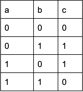
The possible input values in this case are 00, 01, 10, 11. The precomputed output that the 2-bit LUT would have already stored would be: 0110. Now, based on the input combination, the 2-bit LUT will return a single output bit. For instance, if the input combination is 10, the LUT would know to assign the output as 1, as according to the truth table for XOR logic, 10 = 1. If the input combination is 11, the LUT would assign the output as 0, as 11 in this case is equal to 0.
Internal Engineering of a LUT
The LUT is not built from traditional logic gates, but rather from an array of multiplexers. These MUXes select preloaded outputs based on the input combinations. Even though we refer to the LUT as a small block of memory, it is important to keep in mind that its internal hardware is not made up of RAM. Instead, LUTs act like memory using multiplexers that are hardwired to choose between logic values depending on the input.
For instance, if we go back to our 2-input LUT example, we know that our LUT needs to store 4 possible output values: 0110. Internally, this would be handled using a 4:1 MUX. Why? Because we have 4 outputs which will act as inputs in the MUX, and we must return only 1 bit. The select bits in this case would be “a” and “b”(from the truth table). So if my select bits are 00, the MUX will select the first input, D0, which in this case is 0, and return that as the output.
But our example is very niche and not common in the real world. Realistically, LUTs are much larger, and the most common LUT takes in 6 inputs. This means it can implement any logic function of 6 variables by storing 26 = 64 output values. These types of LUTs are internally engineered through an array or tree of 2:1 MUXes.
At each level of the tree, one input bit acts as the select bit to choose between two possible outputs from the previous level. Let’s take a realistic example: I want to implement a function with 6 input variables: A, B, C, D, E, and F. The LUT would store 64 precomputed outputs, which would act as inputs in the MUXes labeled from D0 to D63. The MUX tree will start from the lowest level, and based on the 1-bit select line, it will choose between D0 and D1, and the other MUX between D2 and D3. Keep in mind that each pair is handled by one MUX(hence 2:1), and usually, the least significant input bit is what is used as the select input. In this case, our LSB would be F. So once the first layer of MUXes selects between D0-D3 using F, the outputs from this layer will become the inputs to the next layer of MUXes. The select bit for this layer of MUXes would then be the next LSB, in this case, which would be E.
This hierarchical selection goes on and continues upward throughout the MUX tree. At the final stage, the select input would be A, which is the Most Significant Bit in our case, and now only one output will remain. This would be the final result of the logic function.
HDL to Hardware
Normally, when we are writing code in any HDL like Verilog or VHDL, we are essentially describing logic gates. However, our HDL code, when run on an FPGA, will be translated into LUT-based logic through the synthesis tool. For example, let’s take a look at this Verilog snippet ,which is related to our 2-input LUT example implementing XOR logic from earlier:
assign y = a ^ b;In this Verilog line, we are telling the FPGA that the output Y should be assigned to an XOR b, which will make the synthesis tool take this description and automatically build the according truth table for the XOR function. In our example, the tool will identify that this logic can be implemented using a 2-input LUT, as the logic only depends on two input variables, making it precompute all the possible output combinations of our two inputs. The output combinations would be directly stored into the LUT, and during the FPGA configuration phase, the bitstream file generated by the synthesis tool will load this information into a LUT in the FPGA.
As I mentioned earlier, most FPGAs these days provide 6-input LUTs, meaning a single LUT can implement any logic function of up to 6 input variables. However, the process is still relatively similar to our example. If at all, the logic function requires more than 6 inputs, the synthesis tool will split the function into smaller parts that each separate LUT can handle.
LUTs inside an FPGA
I mentioned earlier about the LUT residing inside a CLB. These CLBs on an FPGA are usually arranged like a grid across the FPGA, and they are connected to each other, which is one of the strong advantages of an FPGA. The CLB is the smallest unit in an FPGA and usually contains one or more LUTs for combinational logic, one or more flip-flops for sequential logic, sometimes a carry chain logic, and multiple MUXes.
When the Verilog code is synthesized, the synthesis tool will map each logic function into one or more LUTs for combinational logic, which are then assigned to available CLBs in the FPGA fabric. The entire FPGA is essentially like a sea of CLBs, where each block can be customized to act as a small piece in your whole logic design. This is what really makes FPGAs “configurable” and changeable, unlike your traditional ASICs.
To wrap it all up, LUTs are one of the key building blocks behind FPGAs. I went over how they store precomputed outputs, how they are built through MUXes, and how your HDL code will get synthesized to act on these LUTs. Keep in mind that LUTs only apply to combinational logic, and inside the CLBs, the flip-flops are in charge of any sequential logic operations, which we will be going over in the next article.
Thanks for reading!